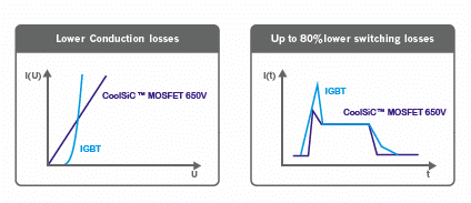
Although silicon carbide-based MOSFETs (SiC) allow for much higher levels of efficiency compared to silicon-based versions (Si), it is not always easy to decide which technology is the best option. In this article, we intend to explain the criteria to be taken into account. For voltages above 1000 V, IGBTs used to be the solution of choice. But the “super properties” of SiC allow for fast-switching unipolar components that can be used instead of bipolar IGBTs. They allow applications that were previously only feasible at lower voltages (<600V) to now be implemented at higher voltages. Compared to bipolar IGBTs, these SiC-based MOSFETs achieve power loss reductions of up to 80 percent.
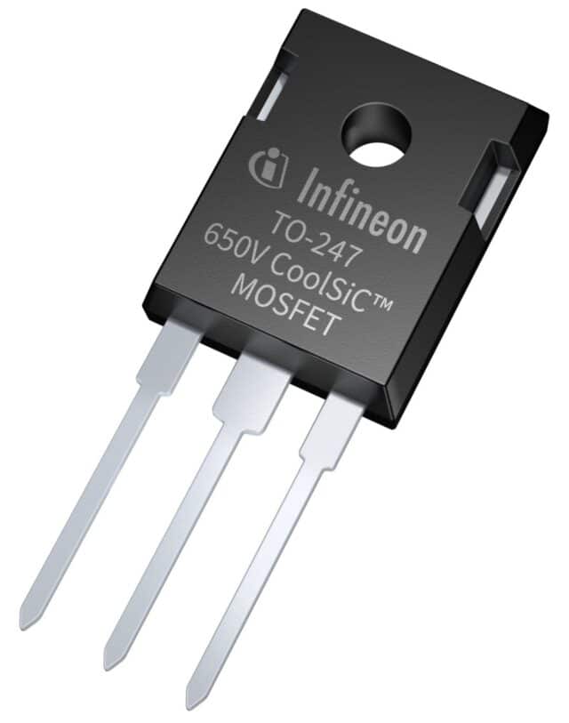
Infineon has further optimized the already beneficial properties of SiC—with CoolSiC Trench Technology, it is possible to build MOSFETs with threshold voltages (Vth) especially high and low Miller capacitance. This makes them more resistant to undesirable parasitic triggering effects relative to other SiC MOSFETs. In addition to models of 1200 and 1700V, Infineon has expanded its catalog by incorporating 650V CoolSiC MOSFETs, which can also be used in applications with a 230 V supply. Its improvements in system efficiency and robustness and its lower cost allow its use in applications such as telecommunications, servers, charging stations for electric vehicles and battery packs. If the choice is generally between the proven Si-based MOSFETs and the newer SiC-based MOSFETs, there are several criteria to consider.
Application power density and efficiency
Compared to silicon, the RDSon Silicon carbide is less prone to volatility in the operating temperature range. With a SiC-based MOSFET, the RDSon only moves by a factor of about 1,13 between 25 and 100 °C, while a typical Si-based MOSFET, such as the coolMOSTM C7 from Infineon, it changes by a factor of 1,67. This means that the operating temperature has much less impact on power loss and can therefore be much higher. As a consequence, SiC-based MOSFETs are especially well-suited for high-temperature applications or can perform with simpler cooling solutions to achieve the same levels of efficiency.
of switching losses with respect to the IGBTs—in this case using the example of the
Infineon 650V CoolSiC MOSFETs.
MOSFET Drivers
When switching from silicon to silicon carbide, the question also arises as to which are the most suitable drivers. If Si-based MOSFET drivers generate a gate voltage of up to 15 V, they can generally still be used. However, a gate drive voltage of up to 18 V allows a significant reduction in resistance RDSon (up to 18 percent at 60 °C), so it's still worth a change of controller.
It is also recommended to avoid negative voltages on the gate, since they can cause a variation in VGS(th), so that the RDSon increase with prolonged operation. Voltage drop across the source inductance in the gate drive loop results in a high di/dt, which can cause a V levelGS(off) negative. An even greater challenge is posed by very high dv/dts, a consequence of the drain capacitance of the gate of the second switch in a half-bridge configuration (half-bridge). This problem can be avoided with a lower dv/dt, but at the expense of reduced efficiency.
The best way to limit the negative gate voltage is to use a separate power supply and driver circuit via the Kelvin source concept and integrate a diode clamping. Located between the gate and the switch source, a diode clamping reduces the negative voltage present on the gate.
Reverse recovery charge Qrr
Especially with resonant topologies or designs that use continuous hard switching of the driver body diode, it is essential to consider the reverse recovery charge Qrr. This is the charge that must be removed from the integrated body diode—present in all diodes—when the diode is no longer conductive. Several component manufacturers have made great efforts to reduce this load as much as possible. The family "Fast Diode CoolMOSInfineon's ” is an example of the fruits of those efforts. These models are characterized by faster body diodes and can lower the Qrr by a factor of 10 compared to its predecessors. Infineon's CoolSiC family offers even more than this—over the latest CoolMOS components, these SiC MOSFETs achieve an additional tenfold improvement.
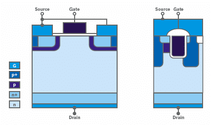
CoolSiC technology supports the development of systems with fewer components and magnetic elements and smaller heat sinks, being simpler, more compact and affordable. Thanks to Trench Technology, these components also guarantee minimal losses in use and maximum reliability in operation.
Power Factor Correction (PFC)
Currently, the focus of the industry is on increasing the efficiency of the system. To achieve efficiency values of at least 98 percent, more efforts are being directed toward power factor correction (PFC). SiC-based MOSFETs with Qrr improved help to achieve the objective. These models now support half-bridge/full-bridge topologies (half-bridge/full-bridge) hard switched for PFC. For its CoolMOS technology, Infineon had previously recommended a “triangle current mode” approach, but with SiC it is possible to implement a continuous conduction mode totem pole PFC.
during the operation.
output capacity COSS
In a hard switched topology, the stored energy E must be dissipatedOSS; this power is typically higher than the latest CoolMOS version. However, compared to the turn-on losses of a totem pole PFC, it still remains relatively low and therefore almost negligible, at least initially. The lower capacitance means that it is possible to benefit from faster switching speeds, but this can also lead to drain source overshoot (VDS) during activation.
With Si-based MOSFETs, this can be compensated for by using an external gate resistor to slow switching speeds to achieve the required 80 percent drain-source voltage limitation. The disadvantage of this solution is that, especially during activation, the increase in current causes an increase in switching losses.
Although the output capacitance with SiC-based MOSFETs is greater than with Si-based power semiconductors across a drain-source voltage of 50 V, the ratio COSS/VDS it's much more linear. The consequence of this is that SiC-based MOSFETs make it possible to use a smaller external resistor in the same circuit than Si-based models, without exceeding the maximum drain-source voltage. This can be an advantage in some circuit topologies, such as LLC resonant DC/DC converters, where the additional gate resistor can be omitted.
Conclusion
Although silicon carbide technology has many advantages, the obsolescence of Si-based MOSFETs is by no means a given. This is due, in part, to the much higher threshold voltage of the body diode—simply replacing a Si-based MOSFET with a SiC-based model would quadruple the power loss in the body diode, essentially sacrificing the efficiency gains. In order to benefit from the superior efficiency of today's SiC-based MOSFETs, the function boost of a PFC should be used across the MOSFET channel and not in the reverse direction of the body diode. Dead times also have to be optimized to take full advantage of the benefits of SiC-based MOSFETs.
SiC-based MOSFETs have lower conductivity losses and up to 80 percent switching losses over IGBTs—in this case using the example of Infineon's 650V CoolSiC MOSFET.
Trench technology minimizes losses during use and provides maximum reliability during operation.
Authors: Hannah Metzner, Product Sales Manager Power of Rutronik, and Rene Mind, Senior Staff Engineer of the PSS Division of Infineon


