MOSFET Switches: Basics and Applications in Power Converters

Get valuable resources straight to your inbox - sent out once per month
We value your privacy
How Does a MOSFET Work
A metal-oxide-semiconductor field-effect transistor (MOSFET) is an electronic device that falls under the category of field-effect transistors (FETs). These devices act as voltage-controlled current sources, and are mainly used as switches or for the amplification of electrical signals. The MOSFET is controlled by applying certain voltage conditions to the gate. When the MOSFET is turned on, current flows from the drain to the source of the MOSFET, through a channel created in the bulk (also called the body). In most cases, the MOSFET’s bulk is connected to the source, which is why MOSFETs are commonly referred to as 3-pin devices.
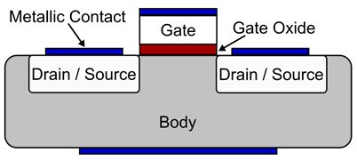
Figure 1: MOSFET
P-Channel MOSFETs vs. N-Channel MOSFETs
MOSFETs are semiconductor-based devices, and are mostly built using either P-type or N-type silicon. The difference between these two silicon types is the charge stored by the dopant ions, which are charged particles that are injected into the silicon to create charge instability, making the element useful for electronic purposes. If an area of silicon has been doped with ions that have five valence electrons (group 5 in the periodic table) then there is an extra electron that is set free into the semiconductor, so the charge will be overall negative (N-type). Since they contribute an electron, these impurities in the silicon are called donor impurities. On the other hand, elements with three electrons in the valence band will be lacking an electron, which is equivalent to contributing a hole, meaning the overall charge will be positive (P-type). These impurities are also called acceptor impurities. Figure 2 shows the difference between P-type and N-type semiconductor dopants, and the effect they have on the silicon structure.
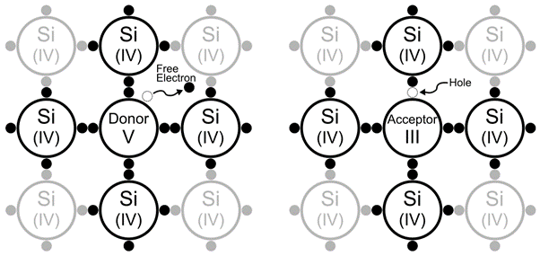
Figure 2: Dopants – Donor vs. Acceptor Impurities
The simplest MOSFET structure is comprised of a substrate, which can be P-type or N-type, and two areas of silicon of the opposite polarity to the bulk, which make up the drain and the source (see Figure 3). MOSFETs can be built to have a P-type substrate and an N-type drain and source regions, which means that in order for current to flow from the drain to the source the channel will also have to be N-type. These are called N-channel MOSFETs, or NMOS transistors. Conversely, if the substrate is N-type, the channel will be P-type, so the MOSFET is called a P-channel MOSFET, or PMOS transistor.
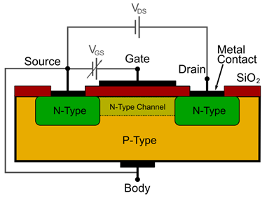
Figure 3: MOSFET Structure
Enhancement vs. Depletion MOSFETs
MOSFETs get their name from the structure through which they are controlled. The gate pin is connected to a conductive electrode, which is separated from the substrate by a layer of silicon oxide or another dielectric material. Therefore, when a voltage is applied to the gate, an electric field is generated from the metallic gate, through the oxide, to the silicon substrate (metal-oxide-semiconductor). This electric field has an effect on the free charge carriers in the substrate semiconductor (e.g. holes or electrons), and pulls them up close to the gate to form a channel or pushes them away to destroy the channel.
When an electric field is applied to a semiconductor, it acts upon the device’s free charge carriers. The free electrons, evenly distributed throughout the semiconductor, are attracted to the electric field’s point of entry (in the case of a MOSFET with a positive gate voltage this is the gate electrode), whereas the holes will be dragged in the direction of the electric field opposite to the electrons (see Figure 4). This is called carrier drift, and logically changes the charge concentration distribution within the semiconductor.
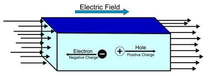
Figure 4: Carrier Drift in Semiconductors
The principal aim of the MOSFET is to control the creation of a channel between the drain and the source, which is done by concentrating the right carriers in the area closest to the gate in order to create or destroy the channel. Therefore, MOSFETs can be distinguished into two basic groups: depletion MOSFETs and enhancement MOSFETs.
Depletion MOSFETS come with a pre-generated channel (see Figure 5). When a voltage is applied to the gate, the electric field pushes out the carriers in the channel, thus depleting it. Therefore, depletion MOSFETs can be equated to a normally closed switch.
In enhancement MOSFETS, the channel only appears when the gate voltage is applied, attracting charges and enhancing the channel region. This type of MOSFET, which can be considered a normally open switch, is most commonly used in electronic applications because if power is lost the switch turns off and current stops flowing in the circuit, which avoids uncontrolled operation and increases circuit safety. The rest of this article will be referring only to enhancement N-channel MOSFETs.
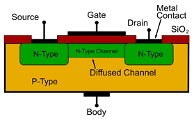
Figure 5: Depletion Mode MOSFET
Figure 6: Enhancement Mode MOSFET
MOSFET Operation Regions
From what has been explained thus far, it is clear that one of the most important aspects in a MOSFET’s operation is the potential voltage applied to the gate. In fact, the MOSFET’s operation is defined by the voltage potential between the MOSFET’s gate and its source (VGS). Figure 7 shows how VGS affects the flow of current through the MOSFET. In an enhancement N-channel MOSFET, when there is no potential voltage between the gate and the source, the channel is nonexistent. This operation region is called the cutoff region; when the transistor is in this operating region, there is no current flowing from drain to source, which means the MOSFET behaves like an open switch.
As the gate voltage increases, the channel starts to form, but it does not enable conduction between the drain and the source until a certain voltage level, called the threshold voltage. Once the threshold is reached, current begins to flow through the MOSFET. This region, called the saturation region, can be compared to a voltage-controlled current source. As the gate voltage increases, so does the current flowing through the switch. This is the region mainly used for signal amplification, since small voltage changes in the gate lead to larger changes in output current (see Figure 7). This current can then be used to change the voltage across a resistor, which is the basis of common-source amplifiers.

Figure 7: Drain Current vs. Gate Voltage
As the gate voltage continues to increase, so does the channel. In the saturation region, the channel still does not fully connect the drain and source regions, so the voltage between the source and drain does not have much of an effect on the operation. However, once the channel has been enhanced enough so that it connects the drain and source (this is called the pinch-off voltage, which is the upper limit of the saturation region), the MOSFET channel is fully enhanced and the transistor behaves as a fully closed switch.
From this point on, the MOSFET can be considered as a resistance, due to the voltage loss between the drain and source (RDS(ON)). This new operation region, called the ohmic or linear region, sees an increase in the current across the MOSFET, which is linearly proportional to the voltage applied between the drain and source of the MOSFET — although this is limited by the gate-source voltage (see Figure 8).
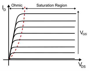
Figure 8: Drain Current vs. Drain-Source Voltage
Figure 8 also gives insight into what operation regions are useful for different applications. As was mentioned previously, the saturation region is the best for amplification, because for the same VDS, a small change in gate voltage causes a much larger change in current. However, because the power consumed by the MOSFET is defined by the product of the current and the voltage across the MOSFET (VDS), the saturation region is also the worst regarding power efficiency, since it has notable current and drain-source voltage.
Therefore, when the MOSFET is used in switching applications, it is imperative to make sure that the MOSEFT only works as a fully open or fully closed switch to reduce power loss. In other words, it must only work in the cutoff or linear regions, and avoid saturation as much as possible.
Parasitic Components in Power MOSFETs
As with any electronic device, it is important to consider the parasitic elements that it incorporates, meaning the components that are unintentionally created by the structure of the device. This article has already talked extensively about one of them, the on resistance, but there are other components embedded in the MOSFET structure (see Figure 9 and Figure 10).
The other main passive components that appear in MOSFETs are the different capacitors created in the transistor’s structure. There are many parasitic capacitors, but the main ones to consider are the capacitors formed between the gate and the drain, and between the gate and the source. These capacitors limit the maximum switching frequency at which the device can operate.
In addition to these passive elements, a BJT is created by the N+-P-N- junctions formed by the source, body, and drift regions. This transistor is critical for safe operation of the MOSFET. If it is accidentally turned on, causes the MOSFET to enter a “latch-up” condition, which significantly decreases the maximum blocking voltage. If this voltage is surpassed, the BJT causes the device to enter avalanche breakdown, which can destroy the device if the current is not limited. Therefore, the BJT must always be turned off by making the voltage at the base (body) as close as possible to the voltage at the emitter (source). This is why the source and the body are nearly always short-circuited in power MOSFETs. However, by shorting the source and bulk regions, a diode is created, known as the body diode. This diode is not as problematic as the BJT, and it can even be useful in some applications.
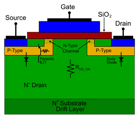
Figure 9: Power MOSFET Parasitic Components
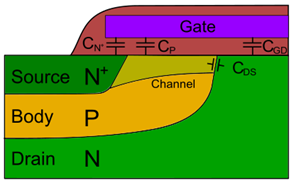
Figure 10: Parasitic Capacitors
Power MOSFETs
One of the aims when designing a MOSFET for power applications is ensuring that it can work at high voltages, meaning that it can block high voltage potentials when required without breaking down. This is achieved via the diode effect that occurs between the N-Si of the drain and the P-Si of the bulk. When biased, the drain-bulk PN junction acts like a reverse-biased diode, creating a spatial charge region (SCR) and blocking the voltage. The higher the voltage bias, the larger the spatial charge region necessary to block the voltage. If the voltage is high enough, the SCR could cross the space between drain and source, which would enable conduction through the MOSFET. This is called reverse breakdown. So, it would seem that the key to working at high voltages is to have a very long MOSFET channel. However, there are two reasons why making longer transistors is not a viable option:
- Efficiency: A longer channel means a higher RDS(ON), which in turn leads to higher conduction losses.
- Size: Longer channels take up more space, reducing the integration capability of the MOSFET.
For this reason, power MOSFETs are not built with the traditional MOSFET structure we are accustomed to seeing (see Figure 5). Instead, power MOSFETs are built with a vertical structure, with the source and gate on the top plate, and the drain on the bottom (see Figure 11).
Since the depth of the transistor is not a problematic production parameter, the depletion region can be as long as necessary, with only the issue of increased conduction loss. By connecting the MOSFET drain to the entire metal backplate, it is also much easier to connect these MOSFETs in parallel to increase current capability.
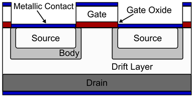
Figure 11: Vertical MOSFET Structure
As mentioned previously, the main energy loss in a MOSFET transistor comes from either switching or conduction. Switching losses can be minimized by having fast-switching transistors and applying soft switching, but reducing conducted emissions depends almost entirely on the structure of the MOSFET, especially on the on resistance, or RDS(ON).
The value of the on resistance depends on the length of the channel and the carrier concentration of the semiconductor. Of course, higher voltages create a stronger electric field, and therefore a larger depletion region (see Figure 12). Since the depletion region must not cross the entirety of the channel, the depth must be made very long. However, increasing the semiconductor length has a significant negative effect on the on resistance, which is why punch-through semiconductors where developed.
In this type of semiconductor device, the N region in the drain is divided into two parts of different doping densities: an N+ region with a very high doping density, and a low-density region. This low-density region is called the drift layer. Due to the doping gradient between these two regions, the electric field generated by the reverse bias is no longer triangular. Instead, it can “punch through” the limit of the drift region, acquiring a rectangular shape (see Figure 13). This allows for higher maximum blocking voltages without having to increase the channel length.
However, the drift layer’s low doping concentration has a negative effect on the semiconductor’s conductivity in that region, limiting the effect on the on resistance.
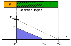
Figure 12: Non-Punch Through
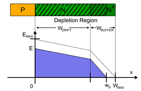
Figure 13: Punch-Through
MOSFET Safe Operating Area (SOA)
Like all devices, MOSFETs have limits to the operating conditions they can work in. These limiting conditions mostly have to do with the maximum voltage and current combinations that they can work with before breaking down. To better show these limitations, most MOSFET datasheets come with a safe operating area (SOA) graph (see Figure 14).
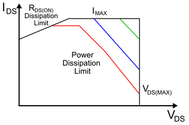
Figure 14: MOSFET SOA
The top limit of the safe operating area is set by the maximum current that can flow through the device. This is limited by the device’s RDS(ON), since the current flowing through the MOSFET channel (and therefore the resistor) generates heat, which can cause the device to break down.
The SOA’s vertical right-side limit is set by the maximum voltage that the MOSFET can block without breaking down and enabling conduction. This is determined by the MOSFET’s structure, the channel length, and the material used in its fabrication, as explained in the previous section of this article.
The diagonal limit in the SOA’s top-right corner represents the MOSFET’s capacity to sustain operation in the saturation region. Due to the combination of current and voltage in the switch, which occurs mainly in saturation, the MOSFET is said to be consuming power, which must then be dissipated in the form of heat. If the product of the current and voltage across the MOSFET is too high, the excessive heat could destroy the device.
The power dissipation limit is represented by several lines in the top-right corner of the SOA. These lines show how the MOSFET’s dissipation limit changes as a function of to the percentage of time that the transistor finds itself in saturation.
If the MOSFET is in DC, then there is a constant current and voltage across the MOSFET, and therefore a constant heating of the device, which greatly limits its capacity to dissipate all the generated energy. However, if the MOSFET is switching on and off, then the device is only being heated for a fraction of the time, and can withstand higher currents and voltages. The shorter the time that it stays on, the higher the voltage and current can be, only limited by the maximum current and voltage.
Conclusion
MOSFETs are an integral part of nearly all electronic systems. Therefore, there is a constant push towards innovating MOSFET structures, discovering new materials and designing circuits with the aim of overcoming current physical limitations while making transistors smaller and smaller. MPS has made significant steps in this field, developing power conversion modules with power switches capable of withstanding up to 100A of continuous current, such as the MPM3695-100. To learn more, visit our website and explore our articles, reference designs, and application notes.
_______________________
Did you find this interesting? Get valuable resources straight to your inbox - sent out once per month!
Technical Forum
 Latest activity a week ago
 3 Comments
Latest activity a week ago
3 Comments
Latest activity 2 weeks ago
2 Comments
3 Comments
Latest activity a week ago
3 Comments
Latest activity 2 weeks ago
2 Comments
Log in to your account
Create New Account