Article

Effect of Intermetallic Compound Bridging on the Cracking Resistance of Sn2.3Ag Microbumps with Different UBM Structures under Thermal Cycling

1
Department of Materials Science and Engineering, National Yang Ming Chiao Tung University, Hsinchu 30010, Taiwan
2
Department of Materials Science and Engineering, National Chiao Tung University, Hsinchu 30010, Taiwan
*
Author to whom correspondence should be addressed.
Metals 2021, 11(7), 1065; https://doi.org/10.3390/met11071065
Submission received: 22 May 2021 / Revised: 23 June 2021 / Accepted: 28 June 2021 / Published: 1 July 2021
(This article belongs to the Special Issue Mechanical Characteristics of Brazed Joints in Metallic Materials)

Abstract

:
In this study, the effect of intermetallic compound (IMC) bridging on the cracking resistance of microbumps with two different under bump metallization (UBM) systems, Cu/solder/Cu and Cu/solder/Ni, under a thermal cycling test (TCT) is investigated. The height of the Sn2.3Ag solders was ~10 µm, which resembles that of the most commonly used microbumps. We adjusted the reflow time to control the IMC bridging level. The samples with different bridging levels were tested under a TCT (−55–125 °C). After 1000 and 2000 TCT cycles (30 min/cycle), the samples were then polished and characterized using a scanning electron microscope (SEM). Before IMC bridging, various cracks in both systems were observed at the IMC/solder interfaces after the 1000-cycle tests. The cracks propagated as cyclic shapes from the sides to the center and became more severe as the thermal cycle was increased. With IMC bridging, we could not observe any further failure in all the samples even when the thermal cycle was up to 2000. We discovered that IMC bridging effectively suppressed crack formation in microbumps under TCTs.

1. Introduction

Currently, three-dimensional integration circuit (3D-IC) technology has become the most promising solution to extend Moore’s law in very large-scale integration (VLSI) circuits, since the current semiconductor technology has approached its physical and economical limit [1,2,3,4,5]. In a 3D-IC, multiple thin silicon chips within through-silicon vias (TSVs) are stacked and connected by various microbumps [5,6,7]. Those microbumps with good reliability are present to provide the chips a connection thanks to their capability to absolve chip warpage [5,6,7]. Many studies reported that the fast interfacial reaction induces intermetallic compounds (IMCs) in the early stage of bonding. It may quickly consume the entire solder in a short time [8,9,10,11,12,13]. Such an IMC will occupy a large solder volume in the microbumps. Furthermore, the entire solder may be fully transformed into an IMC joint during the thermal treatment of semiconductor processing. During such fabrication, several reflow processes are required, and IMC formation is inevitable.
In the past few years, the formation mechanism of IMCs in solder joints has been widely investigated [8,9,10,11,12,13,14,15,16,17,18,19,20,21,22]. Such studies of interfacial IMCs are crucial, since this relates to several reliability issues [16,19,21,23] and the mechanical properties of solder joints [24,25,26]. Many researchers believe that IMCs are brittle and thus not good for 3D-ICs [19,27,28,29,30]. Lee et al. reviewed the physical properties of the most common and important IMCs in solder joints [31]. Four fracture categories were discussed to confirm the brittleness of IMCs. However, they proposed an opposing opinion, stating that IMCs may not as brittle as the other reports believed due to a lack of scientific data [19,27,28,29,30]. Note that IMCs occupy a much higher volume ratio in a microbump than in a flip chip solder joint [32,33,34]. The effect of the solder height on metallurgical reactions has been reported [35,36]. Several issues, including side wetting [36,37], porous Cu3Sn [38], and IMC bridging [39,40,41] have been identified for low bump height solder joints. Thus, the IMC will still dominate the reliability performance of microbumps. To the best of our knowledge, studies on the effect of IMC bridging on the mechanical properties of microbumps are still limited.
In this study, we employed the binary Pb-free solder alloy (Sn2.3Ag) to fabricate microbumps due to its good mechanical properties, non-toxicity, low melting point, high wettability, and conductivity. The effect of IMC bridging on crack formation in microbumps is investigated. We control the reflow time to generate various IMC bridging levels. The samples with different bridging levels were characterized under thermal cycling tests (TCTs) (from −55 °C to 125 °C). Different under bump metallization (UBM) systems before and after the TCT were also investigated. We propose a new viewpoint that the microbumps fully transformed into IMCs could extend the cracking resistance under thermal cycling. The findings of this study are essential for advanced 3D-IC packing technology.

2. Materials and Methods

Two different UBMs electroplated on silicon (Si) substrates, copper (Cu) and nickel (Ni), were used to fabricate the microbumps. A diffusion barrier (100-nm thick Ti film) was first deposited on a Si wafer followed by the sputtering of a 200-nm Cu seed layer. Lithography was then employed to pattern multiple cylinders (100 μm in diameter) prior to the electroplating of UBMs and soldering. The solder alloy (Sn2.3Ag) was deposited on UBMs using electroplating. The solder height was ~5 μm for the two UBM systems. These samples were reflowed at 260 °C for 1 min to ensure good bonding between the solder and UBM after the solder’s electroplating. Note that some IMCs were formed in this stage (the first reflow). From those samples, we fabricated the Cu/solder/Cu and Ni/solder/Cu microbumps.
Due to an ultra-small amount of solder, it was impossible to generate a self-alignment force. Thus, we employed an infrared microscope (IRM) to bond the samples and to lower misalignment during processing. We were able to observe the UBM positions through the Si chips because they could not fully absorb the infrared wavelengths. All bonding processes were conducted with the assistance of the IRM. The hot plate temperature was then increased to 260 °C. A hot flux was provided for 3 min (the second reflow). Using the IRM, an alignment precision of 10 µm could be achieved.
The as-fabricated microbumps were further reflowed (the third reflow) at 260 °C for 0, 5, 10, and 30 min to investigate the effect of IMC bridging on the cracking resistance of the microbumps under thermal cycling. TCTs were performed between −55 °C and 125 °C for a half hour per cycle. A ramp rate of 15 °C per min was set, and the dwell time in the highest and lowest temperatures was 5 min. In this study, the reflow time represented the total reflow time of three reflows. It included a 1-min reflow after electroplating of the solder, a 3 min reflow during bonding, and an additional reflow for IMC bridging. Thus, the reflow times were actually 4 and 34 min. Failure analysis was conducted using a scanning electron microscope (SEM). Energy dispersive X-ray spectroscopy (EDX) was also employed to identify the compositions of the IMCs.

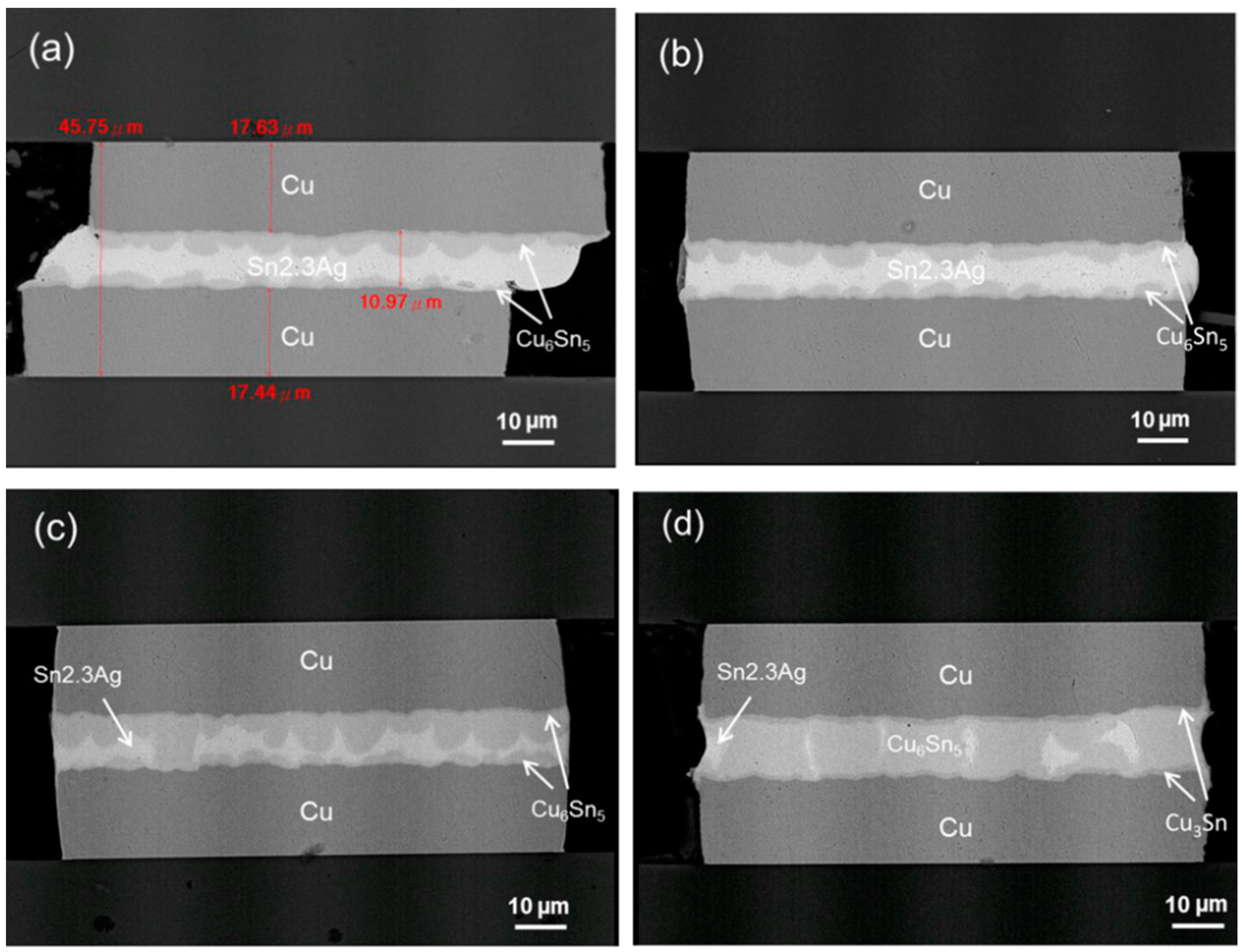
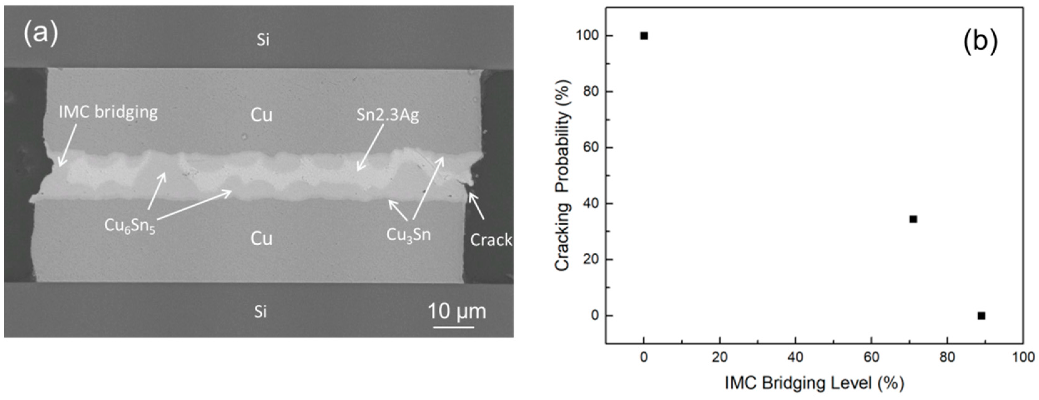
3. Results and Discussion

Figure 1 shows the cross-sectional SEM backscattered images (BEIs) of the Cu/solder/Cu microbumps before and after a TCT. The solder height was ~9–12 µm. In the following analysis, all solder heights were regarded to be 10 µm. Unlike a flip chip structure with organic substrates, our microbumps were fabricated using a chip-to-chip (COC) method. Thus, no significant coefficient of thermal expansion (CTE) mismatch or consequential force was generated from the top or bottom die materials. However, the local CTE mismatches between the Si, UBM, IMC, and solder were still of concern for leading to crack formations, as shown in Figure 1b–d. It is obvious that the scallop-type IMC, Cu6Sn5, quickly formed at both Cu/Si interfaces (Figure 1a). Various cracks formed at the top and bottom IMC–solder interfaces after a 1000-cycle TCT (Figure 1c). Such cracks propagated for some extent as the thermal cycle was increased to 2000. Additionally, some voids also formed at the solder interior after a 1000-cycle TCT. These voids may have reduced the fracture toughness of the solder joints [42]. Such issues should be further investigated. Interestingly, we were able to observe a solder squeezing phenomenon in the 2000-cycle samples. A BEI at a different polished depth after a 1000-cycle TCT is shown in Figure 1b. Various cyclically shaped cracks were detected from the solder surface to its internal structure. These cracks may cause serious reliability problems for the working solder joint in an electronic device.
Note that the CTE and Young’s modulus are very important parameters affecting stress distribution. The large CTE mismatch between the Si (2.6) and the solder (22.2) would cause crack formations during a TCT. The relationship between the critical crack propagation stress (σc) and Young’s modulus can be formulated by the Griffith theory:
σ c = 2 E γ s π a
where a is the haft crack length and γs is the surface energy.
Table 1 shows the CTE and Young’s modulus (E) used in the current study. Note that Young’s modulus can be regarded as the material strength under a TCT. The Young’s modulus of the solder was smallest among the group. Using Equation (1), we could determine that the solder region was the weakest part in the microbump systems. It was definitely the first place where cracks initiated and propagated (Figure 1d).
Ni has been commonly used as a UBM in the semiconductor packaging industry to suppress IMC formation. It has been reported that an interfacial ternary Cu-Sn-Ni compound could form in the Ni region of Pb-free solders [43,44]. However, the effect of such ternary IMCs on the device reliability under a TCT is still unknown. Thus, in this study, Ni/solder/Cu microbumps were also fabricated. Figure 2 shows the typical cross-sectional BEIs of the Ni/solder/Cu microbumps before and after TCTs. It can be seen that a scallop-type (Cu,Ni)6Sn5 IMC formed at the Cu/solder interfaces, and a layer-type (Cu,Ni)6Sn5 IMC formed at the Ni/solder interfaces after the initial bonding process. Various cracks formed at the scallop-type (Cu,Ni)6Sn5 IMC and the solder interfaces after 1000 TCT cycles (Figure 2b). This propagated as the thermal cycles were increased. Most of the cracks were found at the Cu region and solder interfaces (Figure 2b,c). Some cracks appeared at the solder surface. Interestingly, cracks did not form on the Ni side or solder interfaces even after a 2000-cycle TCT (Figure 2c).
In order to control the IMC bridging level, we adjusted the reflow time of the Cu/solder/Cu and Ni/solder/Cu microbumps at 260 °C up to 30 min. Figure 3 and Figure 4 show the typical cross-sectional SEM BEIs of the Cu/solder/Cu and Ni/solder/Cu microbumps reflowed for 5–30 min. The IMC quickly formed at the Cu/solder interfaces due to the fast reaction of the Cu and solder. As is shown in Figure 3, the IMC bridging level increased with an increase in the reflow time. The IMC started to bridge as the reflow time was extended for 5 min (Figure 3b and Figure 4b), and it fully bridged after 30 min (Figure 3d). The dominant IMC phase was Cu6Sn5, with some dielectric layers (Cu3Sn) adjacent to the Cu (Figure 3d). Some solder areas remained intact after a 30-min reflow due to the high concentration of Ag.
Figure 5 shows the cross-sectional BEIs after a 2000-cycle TCT, with fully bridging IMCs in the Cu/solder/Cu and Ni/solder/Cu systems. No sign of cracks in the Cu/solder/Cu system was detected even after a 2000-cycle TCT (Figure 5a). This indicates that the Cu/solder/Cu microbumps with IMC bridging could endure long-term thermal cycling and were effectively resistant to crack formation and propagation.
We also compared the IMC microstructures of the two systems of Cu/solder/Cu and Ni/solder/Cu. We found that the latter one had a non-symmetric structure. A thin and hard Ni UBM layer was observed (Figure 5b). It was expected that stress tended to concentrate at the interface between the layer type (Cu,Ni)6Sn5 (Ni side) and the solder due to the largest CTE mismatch being among these materials, but the cracks were only seen at the IMC/solder interface of the Cu side (Figure 5b). Figure 6 shows the EDX analysis of the IMCs at the Ni and Cu sides of the Ni/solder/Cu microbump after 2000 TCT cycles. It is obvious that the Ni content in the ternary IMCs between the Cu and Ni regions was unequal due to the different diffusion rates of Ni and Cu into the solder. Using EDX, the measured Ni concentrations of the IMCs were 8.97 wt.% for the Ni side (Figure 6a) and 2.48 wt.% for the Cu side (Figure 6b). The Ni concentration (8.97 wt.%) was very close to the maximum solubility of Ni in Cu6−XNiXSn5 calculated by Zeng et al. (8 wt.%) [23]. It has been reported that the stability of the ternary (Cu,Ni)6Sn5 IMC increases with an increasing Ni content [45,46]. The layer type (Cu,Ni)6Sn5 in the Ni side was more thermodynamically stable than the Cu6Sn5. We speculate that the interfacial energy of the Ni side’s IMC/solder interfaces was lower than that of the Cu side’s IMC/solder due to its different Ni content. The interfacial reaction between the Ni UBM and the solder was slower than between the Cu UBM and the solder. Therefore, we did not find any IMC bridging phenomenon until a further 30 min of reflowing (Figure 4d). Similar to the Cu/solder/Cu system, no cracks were found after IMC bridging even after a 2000-cycle TCT. Such microbumps were greatly stable under the TCT and strongly resistant to crack initiation and propagation.
So far, we have discovered that IMC bridging has a major impact on enhancing the cracking resistance under a TCT. Some partial bridging samples were also fabricated to further investigate its failure behaviors. Figure 6a shows a typical cross-section BEI of a 14-min-reflowed Cu/solder/Cu microbump after a 1000-cycle TCT. We can observe partial IMC bridging from the left to the right side. It is obvious that cracks tended to appear and propagate at the non-IMC bridging region rather than at the IMC bridging location (Figure 7a). Additionally, we calculated the IMC bridging level by dividing the IMC-bridged area by its total solder area and plotted it with an observed cracking possibility. The correlation of the observed cracking possibility and the IMC bridging level is shown in Figure 7b. A cracking possibility of 100% with a 0% IMC bridging level indicated that cracks appeared in all non-IMC bridging samples after the TCTs. When the IMC bridging level was about 70%, the possibility of observed cracks significantly dropped to 33%. After raising the IMC bridging level to 90%, the cracking probability reduced to ~0%, indicating no existence of cracks. Generally, the cracking possibility decreased with an increase in the IMC bridging level. We can conclude that IMC bridging effectively inhibited crack initiation and propagation. It thus enhanced the cracking resistance under thermal cycling and prolonged the lifetimes of the microbumps.

4. Conclusions

In summary, the effect of IMC bridging in Cu/solder/Cu and Ni/solder/Cu microbumps on crack formation under a TCT was investigated. We controlled the reflow time to obtain various IMC bridging levels. Without IMC bridging, various cracks formed at the scallop-type IMC–solder interfaces in both systems. These cracks propagated from the outside to the inside as a cyclical shape and turned severely as the thermal cycle was increased. Additionally, we found that the Ni concentration in (Cu,Ni)6Sn5 would also affect the cracking resistance of microbumps under a TCT. The results indicate that IMC bridging and Ni UBM have great impacts on the cracking resistance of the microbumps. They effectively suppress crack formation and propagation.

Author Contributions

Conceptualization, C.-C.M. and C.C.; methodology, C.C.; validation, C.C.; data analysis, C.-C.M., D.-P.T. and C.C.; investigation, C.-C.M. and J.-Y.J.; resources, C.C.; data curation, C.-C.M.; writing—original draft preparation, C.-C.M. and D.-P.T.; writing—review and editing, C.C.; visualization, C.C.; supervision, C.C.; project administration, C.C.; funding acquisition, C.C. All authors have read and agreed to the published version of the manuscript.

Funding

This research was funded by the Center for Semiconductor Technology Research from the Featured Areas Research Center Program within the framework of the Higher Education Sprout Project by the Ministry of Education (MOE) in Taiwan, the Ministry of Science and Technology in Taiwan under grant MOST 110-2634-F-009-027 and the National Science Council of R.O.C. under grants NSC 101-2628-E-009-017-MY3 and NSC 102-2221-E-009-040-MY3.

Institutional Review Board Statement

Not applicable.

Informed Consent Statement

Not applicable.

Data Availability Statement

The data presented in this study are available on request from the corresponding author.

Conflicts of Interest

The authors declare no conflict of interest.

References

  1. Al-Sarawi, S.F.; Abbott, D.; Franzon, P.D. A review of 3-D packaging technology. IEEE Trans. Compon. Packag. Manuf. Technol. Part B 1998, 21, 2–14. [Google Scholar] [CrossRef] [Green Version]
  2. Ladani, L.J. Numerical analysis of thermo-mechanical reliability of through silicon vias (TSVs) and solder interconnects in 3-dimensional integrated circuits. Microelectron. Eng. 2010, 87, 208–215. [Google Scholar] [CrossRef]
  3. Ding, B.; Zhang, Z.-H.; Gong, L.; Xu, M.-H.; Huang, Z.-Q. A novel thermal management scheme for 3D-IC chips with multi-cores and high power density. Appl. Therm. Eng. 2020, 168, 114832. [Google Scholar] [CrossRef]
  4. Ni, T.; Xu, Q.; Huang, Z.; Liang, H.; Yan, A.; Wen, X. Systems. A cost-effective TSV repair architecture for clustered faults in 3D IC. IEEE Trans. Comput. Aided Des. Integr. Circuits 2020. [Google Scholar] [CrossRef]
  5. Jeong, I.H.; Eslami Majd, A.; Jung, J.P.; Ekere, N.N. Electrical and Mechanical Analysis of Different TSV Geometries. Metals 2020, 10, 467. [Google Scholar] [CrossRef] [Green Version]
  6. Rakesh, B.; Mahindra, K.; Goud, M.S.V.; Vignesh, N.A.; Padma, T.; Panigrahy, A.K. Facile approach to mitigate thermal issues in 3D IC integration using effective FIN orientation. Mater. Today Proc. 2020, 33, 3085–3088. [Google Scholar] [CrossRef]
  7. Hachiya, K.; Kurokawa, A. Detecting resistive-open defects of TSVs in power distribution network of 3D-IC. In Proceedings of the 2020 IEEE 24th Workshop on Signal and Power Integrity (SPI), Virtual Conference, 17–20 May 2020; pp. 1–4. [Google Scholar]
  8. Rao, B.C.; Fernandez, D.; Kripesh, V.; Zeng, K. Effect of solder volume on diffusion kinetics and mechanical properties of microbump solder joints. In Proceedings of the 2010 12th Electronics Packaging Technology Conference, Singapore, 8–10 December 2010; pp. 423–428. [Google Scholar]
  9. Choi, W.K.; Kang, S.K.; Shih, D.-Y. A study of the effects of solder volume on the interfacial reactions in solder joints using the differential scanning calorimetry technique. J. Electron. Mater. 2002, 31, 1283–1291. [Google Scholar] [CrossRef]
  10. Huebner, H.; Penka, S.; Barchmann, B.; Eigner, M.; Gruber, W.; Nobis, M.; Janka, S.; Kristen, G.; Schneegans, M. Microcontacts with sub-30 μm pitch for 3D chip-on-chip integration. Microelectron. Eng. 2006, 83, 2155–2162. [Google Scholar] [CrossRef]
  11. Islam, M.; Sharif, A.; Chan, Y. Effect of volume in interfacial reaction between eutectic Sn-3.5% Ag-0.5% Cu solder and Cu metallization in microelectronic packaging. J. Electron. Mater. 2005, 34, 143–149. [Google Scholar] [CrossRef]
  12. Shen, Y.-A.; Ouyang, F.-Y.; Chen, C. Effect of Sn grain orientation on growth of Cu-Sn intermetallic compounds during thermomigration in Cu-Sn2.3Ag-Ni microbumps. Mater. Lett. 2019, 236, 190–193. [Google Scholar] [CrossRef]
  13. Gusak, A.; Tu, K.; Chen, C.J.S.M. Extremely rapid grain growth in scallop-type Cu6Sn5 during solid–liquid interdiffusion reactions in micro-bump solder joints. Scr. Mater. 2020, 179, 45–48. [Google Scholar] [CrossRef]
  14. Chung, C.K.; Duh, J.-G.; Kao, C. Direct evidence for a Cu-enriched region at the boundary between Cu6Sn5 and Cu3Sn during Cu/Sn reaction. Scr. Mater. 2010, 63, 258–260. [Google Scholar] [CrossRef]
  15. Gong, J.; Liu, C.; Conway, P.P.; Silberschmidt, V.V. Initial formation of CuSn intermetallic compounds between molten SnAgCu solder and Cu substrate. Scr. Mater. 2009, 60, 333–335. [Google Scholar] [CrossRef]
  16. Yang, C.; Ren, S.; Zhang, X.; Hu, A.; Li, M.; Gao, L.; Ling, H.; Hang, T. Effect of Sn surface diffusion on growth behaviors of intermetallic compounds in cu/Ni/SnAg microbumps. Mater. Charact. 2020, 159, 110030. [Google Scholar] [CrossRef]
  17. Liu, Y.; Pu, L.; Gusak, A.; Zhao, X.; Tan, C.; Tu, K. Ultra-thin intermetallic compound formation in microbump technology by the control of a low Zn concentration in solder. Materialia 2020, 12, 100791. [Google Scholar] [CrossRef]
  18. Song, R.-W.; Fleshman, C.J.; Chen, H.; Tsai, S.-Y.; Duh, J.-G. Suppressing interfacial voids in Cu/In/Cu microbump with Sn and Cu addition. Mater. Lett. 2020, 259, 126855. [Google Scholar] [CrossRef]
  19. Wu, Y.; Huang, M. Anomalous growth of interfacial intermetallic compounds on (111)-oriented nanotwinned Cu substrate. J. Alloys Compd. 2021, 858, 158340. [Google Scholar] [CrossRef]
  20. Son, J.; Yu, D.-Y.; Kim, M.-S.; Ko, Y.-H.; Byun, D.-J.; Bang, J. Nucleation and Morphology of Cu6Sn5 Intermetallic at the Interface between Molten Sn-0.7 Cu-0.2 Cr Solder and Cu Substrate. Metals 2021, 11, 210. [Google Scholar] [CrossRef]
  21. Rajendran, S.H.; Hwang, S.J.; Jung, J.P. Shear Strength and Aging Characteristics of Sn-3.0 Ag-0.5 Cu/Cu Solder Joint Reinforced with ZrO2 Nanoparticles. Metals 2020, 10, 1295. [Google Scholar] [CrossRef]
  22. Tao, Y.; Xue, S.; Liu, H.; Long, W.; Wang, B. Effect of Cr Addition on Microstructure and Properties of AuGa Solder. Metals 2020, 10, 1449. [Google Scholar] [CrossRef]
  23. Zeng, K.; Tu, K.-N. Six cases of reliability study of Pb-free solder joints in electronic packaging technology. Mater. Sci. Eng. R Rep. 2002, 38, 55–105. [Google Scholar] [CrossRef]
  24. Chen, Y.; Chung, C.; Yang, C.-R.; Kao, C.R. Single-joint shear strength of micro Cu pillar solder bumps with different amounts of intermetallics. Microelectron. Reliab. 2013, 53, 47–52. [Google Scholar] [CrossRef]
  25. Li, D.; Liu, C.; Conway, P.P.J. Microstructure and shear strength evolution of Sn-Ag-Cu solder bumps during aging at different temperatures. J. Electron. Mater. 2006, 35, 388–398. [Google Scholar] [CrossRef]
  26. Ha, S.-S.; Jang, J.-K.; Ha, S.-O.; Yoon, J.-W.; Lee, H.-J.; Joo, J.-H.; Kim, Y.-H.; Jung, S.-B. Effect of multiple reflows on interfacial reaction and shear strength of Sn–Ag electroplated solder bumps for flip chip package. Microelectron. Eng. 2010, 87, 517–521. [Google Scholar] [CrossRef]
  27. Deng, X.; Sidhu, R.; Johnson, P.; Chawla, N. Influence of reflow and thermal aging on the shear strength and fracture behavior of Sn-3.5 Ag solder/Cu joints. Metall. Mater. Trans. A 2005, 36, 55–64. [Google Scholar] [CrossRef]
  28. Wu, C.L.; Huang, M.L. Microstructural evolution of lead-free Sn-Bi-Ag-Cu SMT joints during aging. IEEE Trans. Adv. Packag. 2005, 28, 128–133. [Google Scholar] [CrossRef]
  29. Lu, H.Y.; Balkan, H.; Ng, K.S. Microstructure evolution of the Sn–Ag–y% Cu interconnect. Microelectron. Reliab. 2006, 46, 1058–1070. [Google Scholar] [CrossRef]
  30. Chong, D.Y.; Che, F.; Pang, J.H.; Ng, K.; Tan, J.Y.; Low, P.T. Drop impact reliability testing for lead-free and lead-based soldered IC packages. Microelectron. Reliab. 2006, 46, 1160–1171. [Google Scholar] [CrossRef]
  31. Lee, C.C.; Wang, P.J.; Kim, J.S. Are intermetallics in solder joints really brittle? In Proceedings of the 57th Electronic Components and Technology Conference, Sparks, NV, USA, 29 May–1 June 2007; pp. 648–652. [Google Scholar]
  32. Chen, C.; Yu, D.; Chen, K.-N. Vertical interconnects of microbumps in 3D integration. MRS Bull. 2015, 40, 257–263. [Google Scholar] [CrossRef] [Green Version]
  33. Yang, R.-W.; Chang, Y.-W.; Sung, W.-C.; Chen, C. Precipitation of large Ag3Sn intermetallic compounds in SnAg2.5 microbumps after multiple reflows in 3D-IC packaging. Mater. Chem. Phys. 2012, 134, 340–344. [Google Scholar] [CrossRef]
  34. Chang, Y.; Chen, C.; Chang, T.; Zhan, C.; Juang, J.; Huang, A.T. Fast phase transformation due to electromigration of 18 μm microbumps in three-dimensional integrated-circuit integration. Mater. Lett. 2014, 137, 136–138. [Google Scholar] [CrossRef]
  35. Liu, T.-C.; Huang, Y.-S.; Chen, C. Concentration gradient of Ni in reduced SnAg thickness in Ni/SnAg/Cu microbumps during solid-state aging. ECS Solid State Lett. 2012, 2, P15. [Google Scholar] [CrossRef]
  36. Chuang, H.; Chen, W.; Shih, W.; Lai, Y.; Kao, C. Critical new issues relating to interfacial reactions arising from low solder volume in 3D IC packaging. In Proceedings of the 2011 IEEE 61st Electronic Components and Technology Conference (ECTC), Lake Buena Vista, FL, USA, 31 May–3 June 2011; pp. 1723–1728. [Google Scholar]
  37. Liang, Y.; Chen, C.; Tu, K.-N. Side wall wetting induced void formation due to small solder volume in microbumps of Ni/SnAg/Ni upon reflow. ECS Solid State Lett. 2012, 1, P60. [Google Scholar] [CrossRef]
  38. Lin, J.-A.; Lin, C.-K.; Liu, C.-M.; Huang, Y.-S.; Chen, C.; Chu, D.T.; Tu, K.-N. Formation mechanism of porous Cu3Sn intermetallic compounds by high current stressing at high temperatures in low-bump-height solder joints. Crystals 2016, 6, 12. [Google Scholar] [CrossRef] [Green Version]
  39. Hsiao, H.-Y.; Liu, C.-M.; Lin, H.-w.; Liu, T.-C.; Lu, C.-L.; Huang, Y.-S.; Chen, C.; Tu, K.-N. Unidirectional growth of microbumps on (111)-oriented and nanotwinned copper. Science 2012, 336, 1007–1010. [Google Scholar] [CrossRef] [Green Version]
  40. Huang, Y.; Hsiao, H.; Chen, C.; Tu, K.-N. The effect of a concentration gradient on interfacial reactions in microbumps of Ni/SnAg/Cu during liquid-state soldering. Scr. Mater. 2012, 66, 741–744. [Google Scholar] [CrossRef]
  41. Chiu, W.-L.; Liu, C.-M.; Haung, Y.-S.; Chen, C. Formation of nearly void-free Cu3Sn intermetallic joints using nanotwinned Cu metallization. Appl. Phys. Lett. 2014, 104, 171902. [Google Scholar] [CrossRef]
  42. Zhu, W.; Shi, L.; Jiang, L.; He, H. Effect of intermetallic compound thickness on mechanical fatigue properties of copper pillar micro-bumps. Microelectron. Reliab. 2020, 111, 113723. [Google Scholar] [CrossRef]
  43. Wang, S.; Liu, C. Study of interaction between Cu-Sn and Ni-Sn interfacial reactions by Ni-Sn3.5Ag-Cu sandwich structure. J. Electron. Mater. 2003, 32, 1303–1309. [Google Scholar] [CrossRef]
  44. Wang, S.; Liu, C. Asymmetrical solder microstructure in Ni/Sn/Cu solder joint. Scr. Mater. 2006, 55, 347–350. [Google Scholar] [CrossRef]
  45. Nogita, K.; Nishimura, T. Nickel-stabilized hexagonal (Cu, Ni)6Sn5 in Sn–Cu–Ni lead-free solder alloys. Scr. Mater. 2008, 59, 191–194. [Google Scholar] [CrossRef]
  46. Yu, C.; Liu, J.; Lu, H.; Li, P.; Chen, J. First-principles investigation of the structural and electronic properties of Cu6−xNixSn5 (x = 0, 1, 2) intermetallic compounds. Intermetallics 2007, 15, 1471–1478. [Google Scholar] [CrossRef]
Figure 1. Cross-sectional SEM BEIs of the non-IMC-bridging Cu/solder/Cu microbumps (a) as-fabricated after a TCT for (b) 1000 cycles (edge-polished site), (c) 1000 cycles, and (d) 2000 cycles. Arrows designate the IMCs. SEM: scanning electron microscope. BEI: backscattered electron image. IMC: intermetallic compound. TCT: thermal cycling test.
Metals 11 01065 g001
Figure 2. Cross-sectional SEM BEIs of the non-IMC-bridging Ni/solder/Cu microbumps (a) as-fabricated after a TCT for (b) 1000 cycles and (c) 2000 cycles. Arrows designate the IMCs.
Metals 11 01065 g002
Figure 3. Cross-sectional SEM BEIs of the IMC-bridging Cu/solder/Cu microbumps reflowed for (a) 0 min, (b) 5 min, (c) 10 min, and (d) 30 min. Arrows designate the IMCs.
Metals 11 01065 g003
Figure 4. Cross-sectional SEM BEIs of the IMC-bridging Ni/solder/Cu microbumps reflowed for (a) 0 min, (b) 5 min, (c) 10 min, and (d) 30 min. Arrows designate the IMCs.
Metals 11 01065 g004
Figure 5. Cross-sectional SEM BEIs of the fully IMC-bridging microbumps (reflowed for 30 min) after 2000 TCT cycles. (a) Cu/solder/Cu. (b) Ni/solder/Cu. Arrows designate the IMCs.
Metals 11 01065 g005
Figure 6. EDX (Energy dispersive X-ray spectroscopy) analysis of the IMCs on the (a) Ni and (b) Cu sides of the Ni/solder/Cu microbump after 2000 TCT cycles. The white square indicate the chosen locations for the EDX measurements.
Metals 11 01065 g006
Figure 7. (a) Cross-sectional SEM BEI of the partial IMC-bridging Cu/solder/Cu microbump after a TCT for 1000 cycles and (b) the correlation of the observed cracking possibility and the IMC bridging level. Arrows designate the IMCs.
Metals 11 01065 g007
Table 1. Material properties used in this study. CTE: coefficient of thermal expansion.
SiCuNiCu6Sn5Cu3SnSolder
CTE (ppm/K)2.616.413.416.319.022.2
E (GPa)130.0129.8200.085.685.652.7
Publisher’s Note: MDPI stays neutral with regard to jurisdictional claims in published maps and institutional affiliations.

