MOSFETs and JFETs: Understanding Structures, Differences & Applications
Introduction
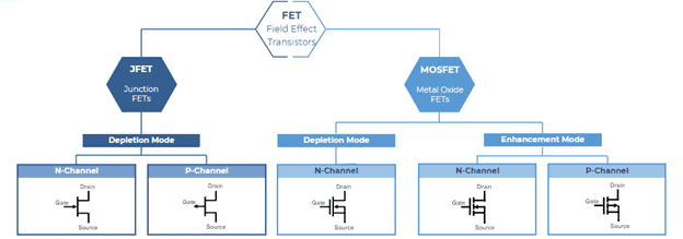
JFET vs. MOSFET structure


Electrical Characteristics
MOSFETs and JFETs are both controlled by the voltage at the gate; however, MOSFETs offer more flexibility when it comes to operation. They can be negatively or positively biased in terms of voltage since they act in both enhancement and depletion modes. In the depletion mode, when no voltage is applied to the gate terminal, the channel shows maximum conductance through the channel. However, if the voltage is either positive or negative, the channel conductivity decreases. This operation is like a JFET; for it to conduct current through its channel, the gate voltage must be at zero, making it a depletion mode device. In the enhancement mode for a MOSFET, when there is no voltage across the gate, the transistor is turned off. When a positive voltage potential is applied, the channel starts conducting, and the MOSFET is operational.
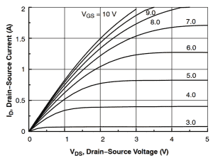
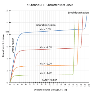
Another major electrical component of any FET is the drain characteristic; this is how you characterize a FET in general and what desired output characteristic you would like to see. These characteristics are controlled by a set of voltages: the gate-source voltage and the drain-source voltage. For JFETs, when the gate-source voltage is zero, there is no current being pushed through the drain-source channel. However, once we apply a drain-source voltage, we see a drain current flow through the channel, which is defined as the ohmic region. With similar reverse biasing, the drain current keeps increasing due to the drain-source voltage, which will eventually have the depletion region constrict in size. This will lead to the pinch off point where our drain current approaches a constant value, and as you further increase your voltage, we will have a roughly constant current, which is designated as the saturation region. Finally, as we keep increasing the drain-source voltage, our JFET loses the ability to resist current, so we have an unimpeded flow of current, meaning our device is in the breakdown region. MOSFETs have a similar drain characteristic, which allows them to act similarly to a JFET in an array of different regions. They have a cut-off region where a MOSFET will be turned off and will have no current flowing. An ohmic region will also exist where the drain current increases with respect to the drain-source voltage. MOSFETs also have a saturation region where the drain current is constant despite an increasing drain-source voltage. However, MOSFETs don’t have the breakdown region that allows for free-flowing current through our device, like a JFET. In terms of electrical capabilities, these two devices are similar in that they both have a variety of uses. A MOSFET has a metal-oxide layer between the gate and the channel, which acts as an insulator and prevents any gate current from flowing. A JFET has a direct junction between the gate and the channel, which allows a small gate current to flow when you reverse bias the device.
Operational differences
Because of how these two FETs are produced, they naturally have some electrical differences from one another. A MOSFET has a lower output impedance than a JFET due to the lower channel resistance. MOSFETs can increase the channel width by applying a positive gate voltage in enhancement mode, while a JFET can only decrease the channel width by applying a negative gate voltage in depletion mode. So naturally, in operation, a JFET will have higher channel resistance when compared to an enhancement-mode MOSFET. In terms of electrostatic discharge, JFETs are less susceptible to ESD damage when compared to MOSFETs. The PN junction acts like a diode that can conduct current in one direction when forward biased and block current in the other direction when reverse biased. The oxide layer acts like a capacitor that can store charge but not conduct current, increasing the gate capacitance. This means that JFETs can withstand higher positive voltages on the gate without damage, as they will simply conduct through the junction without storing extra charge.
Application:
Because of these differences, we tend to use JFETs and MOSFETs in different applications and not necessarily interchangeably. Both JFETs and MOSFETs have a high input impedance, however JFETs have a lower leakage current meaning they draw less current from the input source leading to higher efficiency. This makes them suitable for low-power and high-impedance circuits, such as amplifiers, oscillators, and buffers. JFETs also have lower noise and distortion than MOSFETs, which makes them ideal for audio and signal processing applications. MOSFETs have faster switching speeds and lower output impedance than JFETs, which means they can handle more current and power. This makes them suitable for high-power and low-impedance circuits, such as switches, converters, and regulators. MOSFETs also have a higher frequency response and are more temperature stable in the enhancement mode, which makes them ideal for high-frequency and power electronics applications. In general, MOSFETs will be commonly used in high-frequency applications such as wireless communication devices or RF circuits, power electronic applications, or digital logic circuits. JFETs are used for low-noise applications such as audio amplifiers, analog signal processing, or voltage-controlled resistors.
Characteristics
Low \mathsf{C_{iss}} and \mathsf{C_{rss}}
Can be biased for 0\degree \textsf{TC}
Higher \mathsf{C_{iss}} and \mathsf{C_{rss}}
Additional components required for 0\degree \textsf{TC}
Applications
Trans Impedance Amplifiers TIA
Low \mathsf{R_{ds(on)}} Switch
Conclusion
Overall, both FETs are highly capable and can be used in many different applications and scenarios. There are many differences when considering using a JFET or a MOSFET in terms of cost, modes of operation, electrical properties, structure, and application usage. JFETs and MOSFETs are two types of field-effect transistors that have different ways of controlling the conductivity of the channel. JFET uses an electric field across the reverse biased PN junction, while MOSFET uses a transverse electric field across the insulating layer. MOSFETs have a metal oxide layer for insulation, but JFETs do not. JFETs, however, are cheaper to produce, have a larger gain, and have a flatter characteristic curve than MOSFETs, making them ideal for low-noise and high-impedance applications. But MOSFETs have a higher input impedance and can be used in high-frequency and power applications. Implementation of one of these transistors will ultimately come down to the application you are using it in and the general electrical properties you need to achieve. Both transistors are highly capable and can easily be tweaked, so picking one over the other comes down to the different factors discussed in the article and their general ease of use.
Key Takeaways
- Field-Effect Transistors (FETs) are essential components in electronic circuits for various applications like switching, amplification, filtering, and oscillation.
- FETs come in different types, with MOSFETs and JFETs being the most common. MOSFETs have an oxide layer as an insulator, while JFETs lack this layer.
- Both MOSFETs and JFETs are controlled by the voltage at the gate.
- The electrical characteristics of JFETs and MOSFETs include different regions of operation, such as the ohmic region and saturation region, which affect their performance.
- JFETs have lower input impedance and higher output impedance, making them ideal for low-power and high-impedance applications.
- JFETs are less susceptible to electrostatic discharge (ESD) due to the presence of a PN junction.
- JFETs excel in low-noise and low-distortion scenarios and are often used in audio amplification and analog signal processing.
- Both types of transistors are highly capable and can be used effectively in various electronic circuits, depending on their specific characteristics and applications.