Enhancement MOSFET which is commonly called as E-MOSFET is a type of field effect transistor which is used mainly in voltage-controlled devices. It is a unipolar device, i.e. device in which conduction of current takes place either by electrons or holes. It is a three-terminal device which is mainly used as amplifier or in switching devices. This type of transistor can be used both in analog and digital devices. These transistors are more popular than Bipolar junction transistors due to less power dissipation and negligible leakage current. These are smaller in size and hence find its application in integrated circuits (ICs).
What is E-MOSFET?
The full form of E-MOSFET is Enhancement- Metal Oxide Semiconductor Field Effect Transistor. It is called as enhancement MOSFET because for a creating a conduction channel between drain and source terminal, a positive voltage is required at the gate terminal. Metal is for the metallic contacts that are used to connect drain(D), gate(G) and source(S) terminals. Oxide is for the silicon dioxide (SiO2) layer which is used as an insulating layer between substrate and gate terminal. Semiconductor is for the structure which is used in the construction of this transistor. To sum up, the name E-MOSFET is given to this type of device.

E-MOSFET
Types of E-MOSFET
Based on the type of charge carriers (electrons or holes), E-MOSFET can be classified into two types:
- N-Channel E-MOSFET
- P-Channel E-MOSFET
N-Channel E-MOSFET
This type of MOSFET is called as n-channel MOSFET because the flow of current takes place by conduction of negative charge carriers, i.e., electrons.
Construction of N-Channel E-MOSFET
A n-channel E-MOSFET consists mainly of three terminals: Source(S), Gate(G) and Drain(D). A substrate (SS) is made up of a p-type semiconductor and is internally connected with source terminal or sometimes brought out in a form fourth terminal. The other three terminals, i.e., drain, gate and source as connected to each other by n-doped region through metallic contacts. The figure given below shows the construction of N-Channel E-MOSFET:
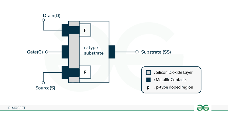
Construction-of-N-Channel-E-MOSFET
Circuit symbol of N-Channel E-MOSFET
Circuit symbol of n-channel E-MOSFET is shown below:

Circuit-symbol-of-n-channel-E-MOSFET
P-Channel E-MOSFET
This type of MOSFET is called as p-channel MOSFET because the flow of current takes place by conduction of positive charge carriers, i.e., holes.
Construction of P-Channel E-MOSFET
A p-channel E-MOSFET consists mainly of three terminals: Source(S), Gate(G) and Drain(D). A substrate (SS) is made up of a n-type semiconductor and is internally connected with source terminal or sometimes brought out in a form fourth terminal. The other three terminals, i.e., drain, gate and source as connected to each other by p-doped region through metallic contacts. The figure given below shows the construction of p-channel E-MOSFET:
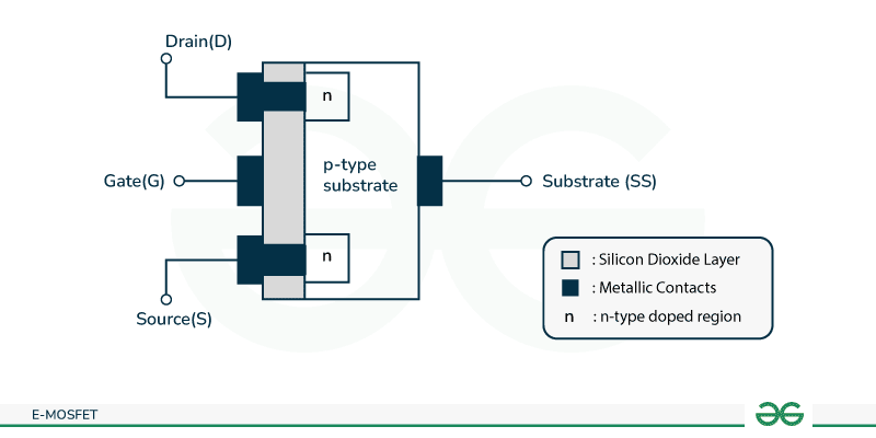
Construction-of-p-channel-E-MOSFET
Circuit symbol of P-Channel E-MOSFET
Circuit symbol of p-channel E-MOSFET is shown below:

Circuit-symbol-of-p-channel-E-MOSFET
Working of E-MOSFET
The working principle of E-MOSFET is that when a positive voltage is applied on the gate terminal, then a conduction channel appears between source and drain terminal.
In n-channel E-MOSFET when the value of gate-to-source voltage is zero, then no drain current flows in a transistor. When the value of gate-to-source voltage is positive then the holes in p-doped region would be repelled by the positive terminal voltage which is applied at gate terminal. By this a depletion region is created near silicon dioxide layer. But, minority charge carriers of substrate, i.e., electrons would be attracted to the gate terminal near the insulating layer of silicon dioxide. When there is increase in positive voltage from gate-to-source terminal, the gathering of electrons near insulating layer of silicon dioxide increases. This results in formation of induced n-channel between n-doped region of drain to source terminal. This induced channel connects drain and source terminals internally and current starts flowing through it. The minimum voltage at which current starts flowing through it is called as threshold voltage (VT).
The working of p-channel E-MOSFET is exactly opposite to that of p-channel E-MOSFET, i.e., all voltage polarities are reversed and thus the flow of current is also reversed.
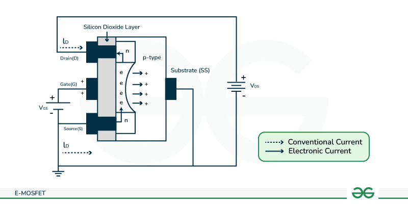
Working-of-E-MOSFET
Characteristics of E-MOSFET
There are two types of characteristics of E-MOSFET- drain characteristics and transfer characteristics. Both type of E-MOSFET, i.e., n-channel E-MOSFET and p-channel E-MOSFET have these characteristics, and are discussed below:
Characteristics of N-Channel E-MOSFET
Characteristics of n-channel E-MOSFET refers to the curves which relate the current and voltage of device with each other. There are mainly two types of characteristics in n-channel E-MOSFET:
- Drain Characteristics: These curves provide the relationship between drain current (ID) and drain-to-source voltage (VDS). When different values of drain current and drain-to-source voltage are plotted on graph, it gives respective values of gate-to-source voltage (VGS). These characteristics are also called as V-I characteristics of a curve.
From the graph shown below, it is observed that when the positive value of VGS is increased, the current ID will also increase. This graph consists of two regions: non-saturated region and saturated region. The non-saturated region of the curve is also called as ohmic region, in this region when drain current is increased then subsequently the value of drain-to-source voltage also increases. Ohmic region lasts till when the value of drain-to-source voltage reaches a threshold value called as threshold voltage (VTN). After this voltage saturation of n-channel E-MOSFET takes place. Hence, the region of curve after threshold voltage is achieved is called as saturated region.

Drain-Characteristics-of-n-channel-E-MOSFET
- Transfer characteristics: These curves provide the relationship between drain current (ID) and gate-to-source voltage (VGS). When different values of drain current and gate-to-source voltage are plotted on X- axis and Y-axis respectively, it provides different values of drain-to-source voltage (VDS). These curves are also called as transconductance curves.
From the transfer characteristics of n-channel E-MOSFET shown below it is observed that when the value of gate-to-source voltage is below the threshold voltage (VTN) then no drain current flows. When gate-to-source voltage is increased, and it reaches to threshold voltage then drain current (ID) starts flowing.

TRANSFER-Characteristics-of-n-channel-E-MOSFET
Characteristics of P-Channel E-MOSFET
Characteristics of p-channel E-MOSFET refers to the curves which relate the current and voltage of device with each other. There are mainly two types of characteristics in p-channel E-MOSFET:
- Drain Characteristics: These curves provide the relationship between drain current (ID) and drain-to-source voltage (VDS). When different values of drain current and drain-to-source voltage are plotted on graph, it gives respective values of gate-to-source voltage (VGS).
From the graph shown below, it is observed that when the negative value of VGS is increased, the current ID will also increase. The graph of p-channel E-MOSFET consists of two regions: non-saturated region and saturated region. The non-saturated region of the curve is also called as ohmic region, in this region when drain current is increased then subsequently the value of drain-to-source voltage also increases. In non-saturated or ohmic region Enhancement MOSFET works as amplifiers. Ohmic region lasts till when the value of drain-to-source voltage reaches a threshold value called as threshold voltage (VTP). After this voltage p-channel E-MOSFET works under saturated region. Hence, the region of curve after threshold voltage is achieved is called as saturated region. In this region Enhancement-MOSFET works as a voltage-controlled resistor.

Drain-Characteristics-of-p-channel-E-MOSFET
- Transfer characteristics: These curves provide the relationship between drain current (ID) and gate-to-source voltage (VGS). When different values of drain current and gate-to-source voltage are plotted on X- axis and Y-axis respectively, it provides different values of drain-to-source voltage (VDS).

TRANSFER-Characteristics-of-p-channel-E-MOSFET
The transfer characteristics of p-channel of Enhancement type MOSFET is the mirror image of transfer characteristics of n-channel E-MOSFET. In this curve the value of drain current increases when the value of gate-to-source voltage decreases.
Difference Between Depletion MOSFET and Enhancement MOSFET
Difference between D-MOSFET (Depletion MOSFET) and E-MOSFET (Enhancement MOSFET) is given below:
|
Parameter
|
Depletion MOSFET
|
Enhancement MOSFET
|
|
Presence of channel
|
Channel is present., either of n-type or p-type.
|
Channel is not present. It is induced during the time of operation.
|
|
Insulating layer
|
Insulating layer of silicon dioxide is presence between gate and channel.
|
Insulating layer of silicon dioxide is present between gate and substrate.
|
|
Working
|
It can work both in depletion and enhancement mode.
|
It works only in enhancement mode.
|
|
Type of transistor
|
It is normally called as ON transistor.
|
It is normally called as OFF transistor.
|
|
Effect of gate voltage
|
Flow of current takes place between source and drain terminal when no voltage is applied at gate terminal.
|
Flow of current does not take place between source and drain terminal when no voltage is applied at gate terminal.
|
Features of E-MOSFET
There are various features of E-MOSFET which makes it different from other types of transistors. Some of such features are discussed below:
- In enhancement MOSFET, channel is not present permanently, but it is induced during the time of working.
- A silicon dioxide layer which acts as an insulator is present between gate and substrate which isolates gate from the main structure.
- Due to the presence of metal-oxide (SiO2) layer input capacitance of enhancement MOSFET is high.
- It is a voltage-controlled device.
- E-MOSFET can be operated at very high frequencies (up to few mega-ohms).
Advantages of E-MOSFET
Enhancement – MOSFET offers many advantages, some of them are listed below:
- As E-MOSFET is a voltage-controlled transistor, so it offers a good control on the conductivity of current across source and drain terminal.
- It could be rapidly turned from off-state to on-state and vice-versa, hence could be used in high-speed switching devices.
- E-MOSFET are small in size, hence it helps in converting a gigantic and bulky device to compact and light-weighted devices.
- E-MOSFET have high reliability as these types of transistors have silicon dioxide layer as an insulating layer which ensure the flow of current through the intended channels.
- These transistors draw very less current from input source and also have a minimal signal loss due to the high input impedance of E-MOSFET.
Disadvantages of E-MOSFET
There are some limitations of using Enhancement – MOSFET, some of them are listed below:
- E-MOSFET have a complex biasing in comparison to other types of transistors.
- E-MOSFET are temperature-sensitive, i.e., change in temperature will affect the working of the transistor.
- These types of transistors are generally costlier than other types of transistors, hence increase the cost of device in which it is used.
- E-MOSFET cannot perform efficiently at high frequencies.
- The properties of E-MOSFET gets altered if the type of semiconductor material is altered.
Applications of E-MOSFET
There are various applications of enhancement MOSFET, some of them are discussed below:
- It is used as an amplifier.
- These types of transistors also find its application in switching devices as it can rapidly be turned on or off when voltage is varied.
- It can also be used for storing memory and hence, finds its application in electronic memory or storage devices.
- E-MOSFETs are used in inverter circuits.
- It is also used in power electronic integrated circuits (IC’s).
Conclusion
Thus, E-MOSFET is a type of transistor that consists mainly of three terminals. It is voltage-controlled semiconductor device. In E-MOSFET as no current flows from drain to source when gate is not supplied with any voltage. So, E-MOSFET is generally called as OFF MOSFET as no current flows from gate to source when gate is applied with zero voltage. It could be used both in analog and digital devices as it offers high input impedance with low power consumption.
Frequently Asked Questions on E-MOSFET
1. What is the full form of E-MOSFET?
The full form of E-MOSFET is Enhancement -Metal Oxide Semiconductor Field Effect Transistor.
2. What is the use of silicon dioxide layer in E-MOSFET?
Silicon dioxide is used in E-MOSFET as an insulating layer between substrate and gate terminal.
3. What is the effect of gate voltage in E-MOSFET?
When the gate terminal is provided with positive voltage, then the conduction between source and drain terminal takes place due to formation of conducting channel in the transistor.
4. What are the types of E-MOSFET?
Based on the channel of the semiconductor E-MOSFET can be classified into two types: n-channel E-MOSFET and p-channel E-MOSFET.
Share your thoughts in the comments
Please Login to comment...