What is Enhancement-mode MOSFET?
MOSFETs are three terminal devices with a Gate, Drain and Source and both P-channel (PMOS) and N-channel (NMOS) MOSFETs are available. The main difference this time is that MOSFETs are available in two basic forms:
- Depletion Type: the transistor requires the Gate-Source voltage, (VGS) to switch the device “OFF”. The depletion mode MOSFET is equivalent to a “Normally Closed” switch.
- Enhancement Type: the transistor requires a Gate-Source voltage, (VGS) to switch the device “ON”. The enhancement mode MOSFET is equivalent to a “Normally Open” switch.
The symbols and basic construction for both configurations of MOSFETs are shown below.
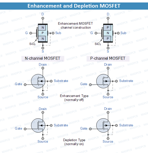
Enhancement and Depletion MOSFET
The more common Enhancement-mode MOSFET or eMOSFET, is the reverse of the depletion-mode type. Here the conducting channel is lightly doped or even undoped making it non-conductive. This results in the device being normally “OFF” (non-conducting) when the gate bias voltage, VGS is equal to zero. The circuit symbol shown above for an enhancement MOS transistor uses a broken channel line to signify a normally open non-conducting channel.
For the n-channel enhancement MOS transistor a drain current will only flow when a gate voltage (VGS) is applied to the gate terminal greater than the threshold voltage (VTH) level in which conductance takes place making it a transconductance device.
The application of a positive (+ve) gate voltage to a n-type eMOSFET attracts more electrons towards the oxide layer around the gate thereby increasing or enhancing (hence its name) the thickness of the channel allowing more current to flow. This is why this kind of transistor is called an enhancement mode device as the application of a gate voltage enhances the channel.
Increasing this positive gate voltage will cause the channel resistance to decrease further causing an increase in the drain current, ID through the channel. In other words, for an n-channel enhancement mode MOSFET: +VGS turns the transistor “ON”, while a zero or -VGS turns the transistor “OFF”. Thus, the enhancement-mode MOSFET is equivalent to a “normally-open” switch.
The reverse is true for the p-channel enhancement MOS transistor. When VGS = 0 the device is “OFF” and the channel is open. The application of a negative (-ve) gate voltage to the p-type eMOSFET enhances the channels conductivity turning it “ON”. Then for an p-channel enhancement mode MOSFET: +VGS turns the transistor “OFF”, while -VGS turns the transistor “ON”.
Enhancement-mode N-Channel MOSFET and Circuit Symbols
Enhancement-mode MOSFETs make excellent electronics switches due to their low “ON” resistance and extremely high “OFF” resistance as well as their infinitely high input resistance due to their isolated gate. Enhancement-mode MOSFETs are used in integrated circuits to produce CMOS type Logic Gates and power switching circuits in the form of as PMOS (P-channel) and NMOS (N-channel) gates. CMOS actually stands for Complementary MOS meaning that the logic device has both PMOS and NMOS within its design.
Enhancement-mode N-Channel MOSFET Amplifier
The DC biasing of this common source (CS) MOSFET amplifier circuit is virtually identical to the JFET amplifier. The MOSFET circuit is biased in class A mode by the voltage divider network formed by resistors R1 and R2. The AC input resistance is given as RIN = RG = 1MΩ.
Metal Oxide Semiconductor Field Effect Transistors are three terminal active devices made from different semiconductor materials that can act as either an insulator or a conductor by the application of a small signal voltage.
The MOSFETs ability to change between these two states enables it to have two basic functions: “switching” (digital electronics) or “amplification” (analogue electronics). Then MOSFETs have the ability to operate within three different regions:
- Cut-off Region: with VGS < Vthreshold the gate-source voltage is much lower than the transistors threshold voltage, so the MOSFET transistor is switched “fully-OFF” thus, ID = 0, with the transistor acting like an open switch regardless of the value of VDS.
- Linear (Ohmic) Region: with VGS > Vthreshold and VDS < VGS the transistor is in its constant resistance region behaving as a voltage-controlled resistance whose resistive value is determined by the gate voltage, VGS level.
- Saturation Region: with VGS > Vthreshold and VDS > VGS the transistor is in its constant current region and is therefore “fully-ON”. The Drain current ID = Maximum with the transistor acting as a closed switch.
MOSFET Summary
The Metal Oxide Semiconductor Field Effect Transistor, or MOSFET for short, has an extremely high input gate resistance with the current flowing through the channel between the source and drain being controlled by the gate voltage. Because of this high input impedance and gain, MOSFETs can be easily damaged by static electricity if not carefully protected or handled.
MOSFET’s are ideal for use as electronic switches or as common-source amplifiers as their power consumption is very small. Typical applications for metal oxide semiconductor field effect transistors are in Microprocessors, Memories, Calculators and Logic CMOS Gates etc.
Also, notice that a dotted or broken line within the symbol indicates a normally “OFF” enhancement type showing that “NO” current can flow through the channel when zero gate-source voltage VGS is applied.
A continuous unbroken line within the symbol indicates a normally “ON” Depletion type showing that current “CAN” flow through the channel with zero gate voltage. For p-channel types, the symbols are exactly the same for both types except that the arrow points outwards. This can be summarized in the following switching table.
| MOSFET Type | VGS = +ve | VGS = 0 | VGS = -ve |
| N-Channel Depletion | ON | ON | OFF |
| N-Channel Enhancement | ON | OFF | OFF |
| P-Channel Depletion | OFF | ON | ON |
| P-Channel Enhancement | OFF | OFF | ON |
So, for n-type enhancement type MOSFETs, a positive gate voltage turns “ON” the transistor and with zero gate voltage, the transistor will be “OFF”. For a p-channel enhancement type MOSFET, a negative gate voltage will turn “ON” the transistor and with zero gate voltage, the transistor will be “OFF”. The voltage point at which the MOSFET starts to pass current through the channel is determined by the threshold voltage VTH of the device.